Thin Film Deposition
Competences and Services
Thin film coatings from the nano- to micrometre scale
SwissNeutronics prepares coatings for science and industry. The deposition process is highly developed to obtain layers with extremely smooth surfaces and homogeneous thickness on large areas. The thin films are coated on substrates with special refined surfaces. Dedicated metrology is applied for the characterisation of coatings and substrates in R&D and production.
Particular highlights are:
Thin film coatings
- Thin film coatings, in particular multilayer coatings in the range of nano- to micrometre
- Metallic coatings: Al, Cr, Fe, FeCoV, Ni, NiCr, NiV, Ta, Ti, TiB2,TiGd, V, Zr; other metals are available on demand
- Metal oxides and nitrides with a defined stoichiometry by employing reactive sputtering
- Non-metallic coatings: C, Si
- Small (few mm²) to large (1100 × 600 × mm²) areas
- Precise and homogeneous layer thickness
- On various substrate materials like glass, ceramics, metals,silicon, etc.
Substrate refinement
- Super-polishing of substrate surface with a roughness <0.2 nm (RMS)
- Formatting of substrates using 5-axis CNC grinding/milling
- Various substrate materials:
| • standard float glass | 0.5–10 mm | 320 × 500 mm² | ||
| • Borofloat®33 | 0.7–15 mm | 320 × 500 mm² | ||
| • DESAG 263T | 0.2–0.5 mm | 300 × 420 mm² | ||
| • N-BK7 | 2.5–30 mm | 320 × 500 mm² | ||
| • silicon wafer | 0.1–1 mm | Ø 300 mm (dependent on thickness) | ||
| • aluminium | 6–30 mm | 200 × 500 mm² |
Other materials, thicknesses or formats may be available on demand.
Surface and interface characterisation
| • Neutron reflectometry | |||
| • Layer thickness | • Layer-resolved magnetisation | ||
| • Interface roughness | • Access to buried layers | ||
| • X-ray reflectometry and diffraction | |||
| • Layer thickness | • Texture | ||
| • Interface roughness | • Access to buried layers | ||
| • Atomic force microscopy | |||
| • Surface roughness | • Topography | ||
| • White light interferometry | |||
| • Surface roughness | • Planarity (figure error) | ||
| • Long-range profilometry | |||
| • Planarity (figure error) | |||
| • Stylus profilometry | |||
| • Internal stress of coatings | • Layer thickness | ||
| • DC Magnetometry | |||
| • Bulk magnetisation | |||
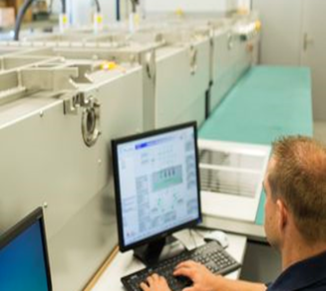
Equipment
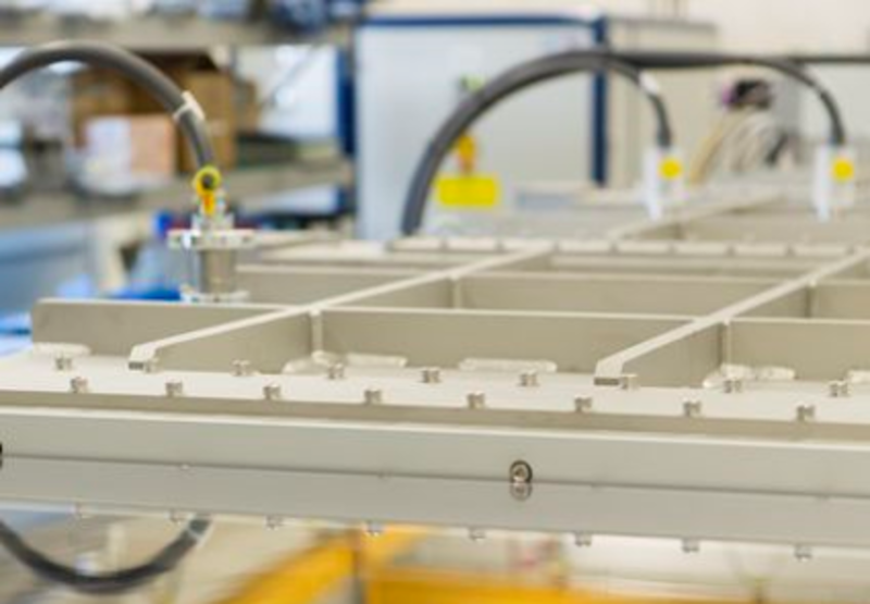
Coating facilities
- 2 inline DC magnetron sputter facilities (types Z900, Z600)
| Z900 | Z600 | ||
|---|---|---|---|
| Coating area | 1100 mm × 600 mm | 540 mm × 420 mm | |
| Number of magnetrons | 4 | 3 | |
| Homogeneityof layer thickness | ±1% | ±1% | |
| Typical layer thickness | 1 nm to 10 μm | 1 nm to 10 μm | |
| Reactive sputtering | N2 and O2; H2 on demand | N2 and O2; H2 on demand |
Equipment for substrate refinement
- 1 polishing machine for surface finish (super-polishing)
- typical format: 320 × 500 mm²
- 2 CNC 5-axis milling/grinding machines
- maximum length: 600 mm
- typical format: 320 × 500 mm²
- accuracy: 0.005 mm
Instrumentation for characterisation of
substrates and coatings
- Neutron reflectometer (NARZISS @ SINQ)
- X-ray powder diffractometer (Siemens D500)
- Atomic force microscope (Nanosurf Easyscan)
- White light interferometer (Zygo)
- Long-range profilometer
- Stylus profilometer (Dektak Surface Profiler)
- Magnetometer (Quantum Design PPMS)
Contact person

SwissNeutronics AG
Bruehlstrasse 28
CH-5313 Klingnau
Switzerland
Dr. Michael Schneider
michael.schneider(at)swissneutronics.ch
phone +41 (0)56 245 02 76
